PASSBAND
(MHz)
fco, MHz
Nom.
STOP BAND
(MHz)
VSWR (:1)
Passband
POWER
INPUT*
(W)
MARKING
NO. OF
SECTIONS
(loss < 1 dB)
(loss 3 dB)
fr20 dB
Typ.
Typ.
( > 20 dB)
Typ.
Typ.
DC-3300
4100
5600
10000
1.2
10
LF9
7
* Derate linearly to 4W at 100
∞
C ambient.
A
B
C
D
E
F
G
H
.150
.150
.028
--
--
.035
.028
--
3.81
3.81
0.71
--
--
0.89
0.71
--
J
K
L
M
N
P
wt
.060
.030
.184
.050
.075
.044
grams
1.52
0.76
4.67
1.27
1.91
1.12
0.15
50
DC to 3300 MHz
Low Pass Filter
LFTC-3300+
LFTC-3300
Maximum Ratings
Operating Temperature
-55∞C to 100∞C
Storage Temperature
-55∞C to 125∞C
Electrical Specifi cations (T
AMB
=25
∞
C)
INTERNET http://www.minicircuits.com
P.O. Box 350166, Brooklyn, New York 11235-0003 (718) 934-4500 Fax (718) 332-4661
Distribution Centers
NORTH AMERICA 800-654-7949 ∑ 417-335-5935 ∑ Fax 417-335-5945 ∑ EUROPE 44-1252-832600 ∑ Fax 44-1252-837010
Mini-Circuits
Æ
Mini-Circuits ISO 9001 & ISO 14001 Certified
REV. H
M107209
LFTC-3300
EDB-020617
AD/YB/CP/AM
060908
Typical Performance Data at 25
∞
C
LFTC-3300
INSERTION LOSS
0
10
20
30
40
50
0
2000
4000
6000
8000
10000
FREQUENCY (MHz)
INSERTION LOSS (dB)
Features
∑ miniature size, 0.15"X0.15"X0.028"
∑ low profi le, 0.028" height
∑ excellent power handling, 10W
∑ hermetically sealed
Applications
∑ harmonic rejection
∑ internal rejection
∑ receivers & transmitters
Ceramic
LFTC-3300
VSWR
1
10
100
1000
0
2000
4000
6000
8000
10000
FREQUENCY (MHz)
VSWR
electrical schematic
typical frequency response
Frequency
(MHz)
Insertion Loss
(dB)
VSWR
(:1)
Outline Dimensions ( )
inch
mm
Outline Drawing
RF IN
2**
RF OUT
5**
GROUND 1,3,4,6
Pin Connections
Demo Board MCL P/N: TB-233
Suggested PCB Layout (PL-112)
** RF IN & RF OUT can be interchanged
RF IN
RF OUT
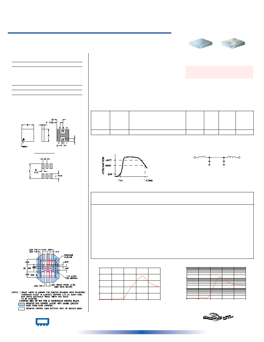
R 20dB
co
f
f
20dB
3dB
40dB
ATTENUATION
CASE STYLE: FR933
PRICE: $3.75 ea. QTY. (10-49)
+ RoHS compliant in accordance
with EU Directive (2002/95/EC)
The +Suffi x identifi es RoHS Compliance. See our web site
for RoHS Compliance methodologies and qualifi cations.
100.00
0.08
1.05
1000.00
0.29
1.24
1600.00
0.34
1.10
2000.00
0.44
1.15
2600.00
0.60
1.21
3200.00
0.76
1.15
3500.00
0.95
1.14
4100.00
2.83
3.16
4600.00
10.72
16.69
5000.00
16.54
44.51
5600.00
24.07
118.44
7000.00
36.57
38.64
8000.00
27.88
23.45
9000.00
22.32
22.03
10000.00
19.50
21.00
PCB Land Pattern
Suggested Layout,
Tolerance to be within
±
.002